
Scale-Up Interconnects: NVLink, NVSwitch, and Ultra-High-Bandwidth Node Fabrics
Why PCIe chokes multi-GPU Tensor Parallelism, how NVLink climbs to 3.6 TB/s, and how NVSwitch SHARP turns 72-GPU racks into one unified compute fabric.

Series: Part 13 of GPU Architecture, Scale-Up Interconnects, and AI Datacenter Infrastructure Series | (Previous) The CUDA Revolution III: Asynchronous Execution, Streams, Graphs, and Driver Ecosystem | (Next) GPU Server Chassis & Tray Architecture: HGX Boards, Compute Trays, and Switch Trays
Summary
Modern frontier AI models have outgrown the physical limits of any single piece of silicon. Even with HBM3e and HBM4 stacks delivering hundreds of gigabytes of memory per package, a 1.8-trillion-parameter Mixture-of-Experts model—plus its optimizer states or multi-hundred-thousand-token KV cache—simply cannot fit on one GPU. Splitting a single model across multiple GPUs using Tensor Parallelism (TP) and Expert Parallelism (EP) solves the capacity wall, but it introduces a brutal synchronization tax: every transformer layer must pause and exchange partial activations across GPUs hundreds of times per second.
In Part 13 of our GPU Architecture, Scale-Up Interconnects, and AI Datacenter Infrastructure Series, we examine the high-speed scale-up fabric that turns a cluster of independent GPUs into one giant logical processor. We trace why standard PCIe Gen 5 and Gen 6 host buses collapse under Tensor Parallelism, follow the evolution of NVIDIA NVLink from 160 GB/s on Pascal to 1.8 TB/s on Blackwell and 3.6 TB/s on Vera Rubin, dissect NVSwitch non-blocking silicon crossbars across 8-GPU HGX baseboards and 72-GPU NVL72 racks, and show how SHARP in-network computing halves collective fabric traffic inside the switch ASIC itself.
Prior Reading Material
To connect scale-up fabrics to the GPU die, memory hierarchy, and distributed serving architectures beneath them, explore these prerequisite deep dives:
- GPU Memory Hierarchy: Registers, Shared Memory, L1/L2, and HBM3e/HBM4 — Part 9: On-chip SRAM vs. stacked HBM bandwidth, and why memory capacity dictates multi-GPU sharding.
- Advanced Packaging & The Chiplet Era: CoWoS, 3D Stacking, and Interposers — Part 7: How silicon interposers and dual-reticle packaging pack maximum HBM beside compute dies before hitting package limits.
- The Tensor Core Revolution: From FP32 Matrix Multiplication to FP4/FP8 Acceleration — Part 8: Why ultra-fast matrix engines starve whenever interconnects lag behind compute throughput.
- vLLM on NVIDIA Vera Rubin: 7.8x Throughput, HBM4 Memory Hierarchy, and the NVL72 Inference Leap — Rack-scale NVL72 serving economics, HBM4 memory tiers, and NVLink 6 throughput in production.
- Disaggregated Inference: Separating Prefill and Decode Nodes at Scale — How high-bandwidth fabrics enable KV cache handoff and phase-isolated LLM clusters.
1. The Single-GPU Memory Wall
For two decades, GPU scaling followed a straightforward script: shrink the transistor node, widen the die up to the photolithography reticle limit, and attach faster memory. Even with CoWoS advanced packaging stitching dual compute dies and eight or more HBM stacks onto a single interposer, a single GPU package remains capped at roughly 192 GB to 288 GB of HBM3e (on Hopper H200 and Blackwell B200/GB200), scaling toward 288 GB+ of HBM4 on Vera Rubin.
Frontier models blow past that ceiling:
- Model Weights: A 1.8-trillion-parameter Mixture-of-Experts (MoE) model stored in BF16/FP16 requires roughly 3.6 TB just for static weights, or ~900 GB even when aggressively quantized to FP4.
- Training States: Full-precision optimizer states, gradients, and activations multiply that footprint by 4x to 8x during pre-training.
- Long-Context KV Cache: Serving concurrent 128K–1M token agentic sessions consumes tens to hundreds of gigabytes of dynamic KV cache per batch.
Because one GPU cannot hold the model, engineers shard individual matrix multiplications across 8, 16, or 72 GPUs. The moment you shard a single transformer layer across multiple GPUs, the interconnect—not the Tensor Cores—becomes the primary determinant of tokens per second.
2. Why PCIe Gen 5 and Gen 6 Bottleneck Tensor Parallelism
Every standard server GPU sits in a PCI Express (PCIe) slot designed to connect peripherals (NICs, NVMe drives, GPUs) to a host CPU root complex. PCIe is engineered for general-purpose I/O compatibility, not tightly coupled collective math:
- PCIe Gen 5 (x16): Operates at 32 GT/s per lane, delivering roughly 64 GB/s per direction (128 GB/s bidirectional).
- PCIe Gen 6 (x16 PAM4): Doubles signaling to 64 GT/s per lane, reaching 128 GB/s per direction (256 GB/s bidirectional, or ~236–240 GB/s usable payload after Flit and FEC overhead).
Why is 128 GB/s to 256 GB/s fatal for Tensor Parallelism (TP)?
In Tensor Parallelism, each GPU computes only a slice of a layer’s attention heads and MLP columns. Before the next layer can begin, every GPU must combine its partial output vector with every other GPU via an All-Reduce collective operation—twice per transformer layer (once after self-attention, once after the MLP block). Across an 80-layer model, a single forward pass triggers 160 synchronous All-Reduce barriers.
If those 160 barriers run over PCIe Gen 5:
- Order-of-Magnitude Bandwidth Gap: A Blackwell GPU’s HBM3e delivers 8 TB/s of local memory bandwidth, while PCIe Gen 5 x16 delivers 64 GB/s unidirectional—a 125x cliff.
- Root-Complex & Switch Tree Contention: Traffic often traverses shared upstream PCIe switches or crosses CPU sockets over UPI/QPI links, adding microseconds of protocol overhead to every hop.
- Idle Tensor Cores: Your Streaming Multiprocessors (SMs) finish their matrix multiply in microseconds and then sit idle for milliseconds waiting on PCIe transfers.
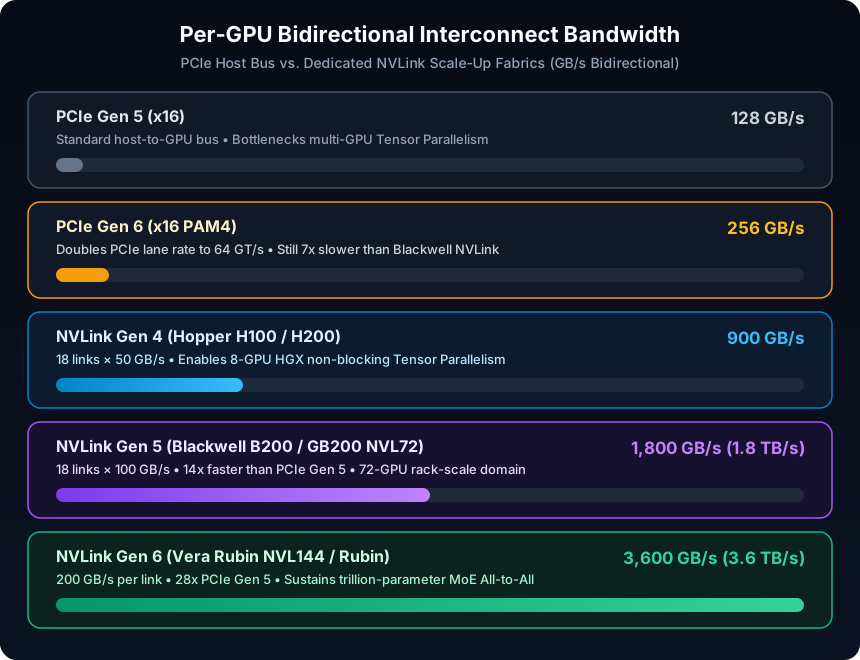 Figure 1: Comparison of per-GPU bidirectional bandwidth across PCIe Gen 5/6 host buses and dedicated NVLink Gen 4–6 scale-up fabrics. Source: Specifications adapted from PCI-SIG and NVIDIA Blackwell / Vera Rubin architecture briefs.
3. The Evolution of NVLink (Gen 1 to Gen 6/7)
To eliminate the PCIe bottleneck, NVIDIA bypassed the host CPU bus entirely and built NVLink—a dedicated, energy-efficient, point-to-point high-speed SerDes interconnect engineered specifically for GPU-to-GPU memory semantics (load/store, atomics, and direct peer-to-peer DMA).
Over six generations, per-GPU bidirectional NVLink bandwidth has roughly doubled every architecture cycle:
| NVLink Generation | GPU Architecture | Release Year | Per-GPU Bidirectional Bandwidth | Key Domain Milestone |
|---|---|---|---|---|
| NVLink Gen 1 | Pascal (P100) | 2016 | 160 GB/s | First 4-link SXM mezzanine interconnect |
| NVLink Gen 2 | Volta (V100) | 2017 | 300 GB/s | 6 links × 50 GB/s; Hybrid Cube-Mesh DGX-1 |
| NVLink Gen 3 | Ampere (A100) | 2020 | 600 GB/s | 12 links × 50 GB/s; 2nd-gen NVSwitch HGX A100 |
| NVLink Gen 4 | Hopper (H100 / H200) | 2022 | 900 GB/s | 18 links × 50 GB/s; 3rd-gen NVSwitch + SHARP |
| NVLink Gen 5 | Blackwell (B200 / GB200) | 2024 | 1,800 GB/s (1.8 TB/s) | 18 links × 100 GB/s; 72-GPU NVL72 rack fabric |
| NVLink Gen 6 | Vera Rubin (Rubin) | 2026 | 3,600 GB/s (3.6 TB/s) | 200 GB/s per link; 260 TB/s rack-scale fabric |
Note: NVIDIA has also previewed 7th-generation NVLink on its post-Rubin roadmap to continue scaling per-link SerDes speeds for multi-trillion-parameter MoE and disaggregated inference domains.
Under the hood, NVLink achieves this throughput by stripping out PCIe’s heavy host-compatibility layers and running tightly synchronized differential pairs directly between GPU packages and switch silicon:
flowchart TD
    A["GPU Tensor Core / SM Memory Request"] --> B["NVLink Transport & Packetizer (Load/Store/Atomic)"]
    B --> C["High-Speed SerDes Lanes (100–200 GB/s per Link)"]
    C --> D["PCB Traces or Passive Twinax Copper Backplane"]
    D --> E["NVSwitch Non-Blocking Silicon Crossbar"]

    style A fill:#0d1b2e,stroke:#38bdf8,stroke-width:2px,color:#f8fafc
    style B fill:#16112e,stroke:#a855f7,stroke-width:2px,color:#f8fafc
    style C fill:#0b221e,stroke:#10b981,stroke-width:2px,color:#f8fafc
    style D fill:#1e293b,stroke:#94a3b8,stroke-width:2px,color:#f8fafc
    style E fill:#082f49,stroke:#38bdf8,stroke-width:2px,color:#f8fafc
Figure 2: Vertical execution path of an NVLink memory transaction from a GPU Streaming Multiprocessor through SerDes lanes to the NVSwitch crossbar.
4. NVSwitch Silicon Crossbars & Non-Blocking Topologies
Having fast links between two GPUs is only half the battle. How do you wire 8 GPUs—or 72 GPUs—so every chip can talk to every other chip simultaneously without traffic jams?
- Why Direct Meshes Hit a Wall: Early 4-GPU and 8-GPU systems (like DGX-1) used point-to-point NVLink bridges in a Hybrid Cube-Mesh. At 8 GPUs, a true all-to-all direct mesh requires 28 separate physical connections, and not every GPU has enough SerDes pins to dedicate direct lanes to 7 peers simultaneously. Some pairs end up 2 hops apart, creating uneven latency and congestion.
- 8-GPU HGX NVSwitch Crossbar (
H100 / H200 / B200): To solve this, NVIDIA introduced NVSwitch—a dedicated, ultra-high-radix silicon switch ASIC soldered directly onto the HGX baseboard. Instead of wiring GPUs to each other, all 8 SXM GPUs wire their NVLink lanes into a bank of NVSwitch chips. The result is a 1-hop, non-blocking all-to-all crossbar: GPU 0 can stream to GPU 7 at full 900 GB/s (Hopper) or 1.8 TB/s (Blackwell) at the exact same instant GPU 1 streams to GPU 6, with zero contention. - Rack-Scale GB200 / GB300 NVL72 Domain: Blackwell takes the HGX crossbar out of a single 8-GPU box and stretches it across an entire liquid-cooled rack. An NVL72 rack houses 18 compute trays (each carrying 4 Blackwell GPUs and 2 Grace CPUs, totaling 72 GPUs) plus 9 NVSwitch trays in the center of the rack. Instead of optical transceivers, over 5,000 passive copper twinax cables sit in a blind-mate copper backplane cartridge, linking all 72 GPUs into a single 130 TB/s non-blocking NVLink domain with up to 13.8 TB to 20.7 TB of unified HBM3e. To software like NCCL and PyTorch, all 72 GPUs behave like one colossal virtual GPU.
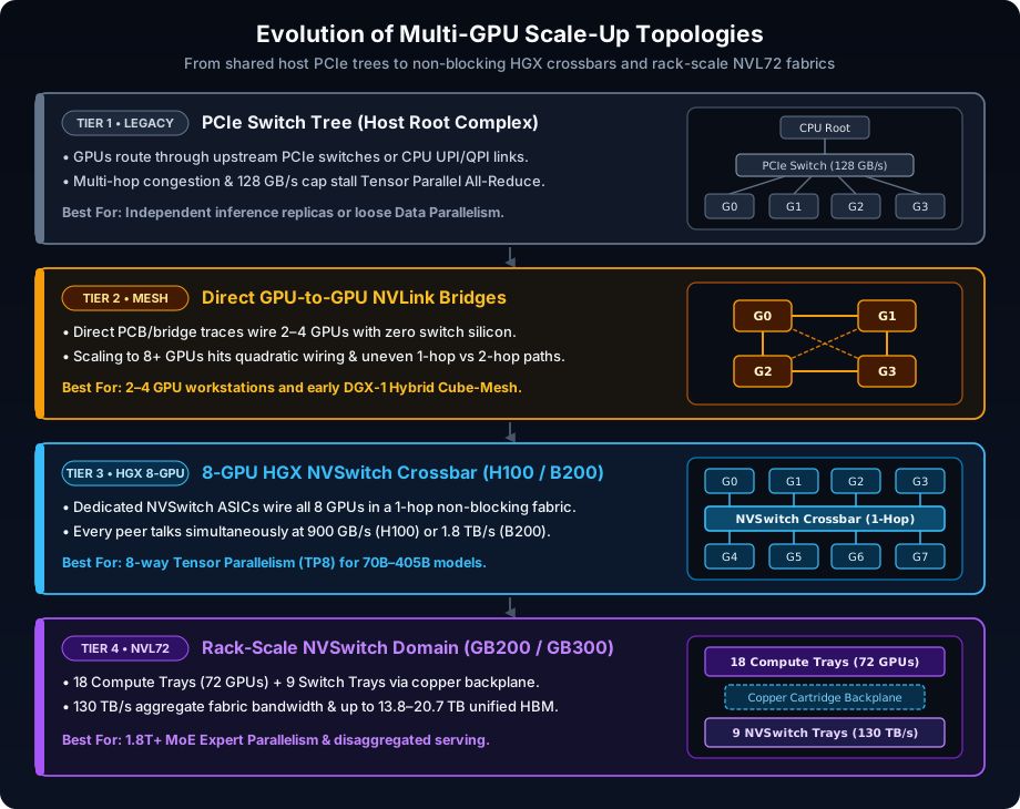 Figure 3: Architectural progression from bottlenecked PCIe switch trees and direct meshes to 8-GPU HGX crossbars and 72-GPU rack-scale NVL72 domains. Source: Topology adapted from NVIDIA HGX and GB200 NVL72 technical documentation.
5. SHARP In-Network Computing (NVLS)
Even with a 1.8 TB/s NVLink 5 crossbar, performing a standard Ring All-Reduce across 8 or 72 GPUs wastes both link bandwidth and GPU compute cycles:
- Standard Ring All-Reduce (
2xTraffic): Every GPU slices its tensor, passes slices around a logical ring in aReduce-Scatterphase (using GPU SMs to sum incoming numbers), and then passes the reduced slices around the ring a second time in anAll-Gatherphase. That moves nearly 2x the payload size across the fabric and scales linearly in hop latency as the GPU count grows. - NVSwitch SHARP (
NVLS,~1xTraffic): Starting with 3rd-gen NVSwitch on Hopper and expanding on Blackwell NVL72, NVIDIA embedded SHARP (Scalable Hierarchical Aggregation and Reduction Protocol) hardware ALUs directly inside the NVSwitch ASIC. Each GPU writes its tensor once into the switch crossbar; the NVSwitch silicon sums the incoming streams in-flight at wire speed and multicasts the single reduced result back to every GPU simultaneously.
The payoff is immediate: SHARP delivers 2x effective All-Reduce bandwidth, keeps collective latency nearly flat whether you synchronize 8 GPUs or 72 GPUs, and frees 100% of the GPU Streaming Multiprocessors to stay focused on Tensor Core math.
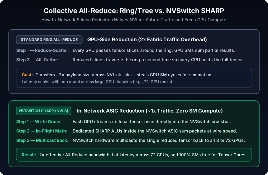 Figure 4: Comparison of GPU-side Ring All-Reduce versus NVSwitch SHARP in-network reduction (
NVLS), showing how switch-resident ALUs halve fabric traffic. Source: Adapted from NVIDIA NCCL and SHARP v3/v4 architecture documentation.
6. Hands-On Simulator: Modeling PCIe vs. NVLink vs. SHARP Latency
To see how these numbers compound across an 80-layer frontier Transformer (which executes 160 All-Reduce barriers per forward pass), you can run the zero-dependency Python simulator below (scripts/nvlink_allreduce_sim.py).
Click to expand runnable code script
"""Simulate All-Reduce collective latency across PCIe Gen 5, NVLink Gen 5, and NVSwitch SHARP."""


def simulate_allreduce(
    name: str,
    num_gpus: int,
    tensor_mb: float,
    bw_unidir_gb_s: float,
    hop_latency_us: float,
    sharp_enabled: bool = False,
) -> dict:
    payload_bytes = tensor_mb * 1024 * 1024
    if sharp_enabled:
        traffic_factor = 1.0
        steps = 2  # Write once to NVSwitch + multicast reduced tensor back
    else:
        traffic_factor = 2.0 * (num_gpus - 1) / num_gpus
        steps = 2 * (num_gpus - 1)

    effective_bytes = payload_bytes * traffic_factor
    bw_bytes_per_us = (bw_unidir_gb_s * 1e9) / 1e6
    transfer_us = effective_bytes / bw_bytes_per_us
    protocol_us = steps * hop_latency_us
    total_us = transfer_us + protocol_us

    return {
        "fabric": name,
        "gpus": num_gpus,
        "traffic_factor": round(traffic_factor, 2),
        "transfer_us": round(transfer_us, 1),
        "protocol_us": round(protocol_us, 1),
        "total_us": round(total_us, 1),
    }


if __name__ == "__main__":
    # 128 MB activation tensor across an 80-layer Transformer (160 All-Reduces per pass)
    tensor_mb = 128.0
    layers_allreduce_count = 160

    scenarios = [
        ("PCIe Gen 5 x16 (Ring, 8 GPUs)", 8, 64.0, 2.5, False),
        ("NVLink Gen 4 HGX (Ring, 8 GPUs)", 8, 450.0, 0.7, False),
        ("NVLink Gen 5 HGX (Ring, 8 GPUs)", 8, 900.0, 0.5, False),
        ("NVLink Gen 5 HGX + SHARP (8 GPUs)", 8, 900.0, 0.5, True),
        ("NVLink Gen 5 NVL72 (Ring, 72 GPUs)", 72, 900.0, 0.6, False),
        ("NVLink Gen 5 NVL72 + SHARP (72 GPUs)", 72, 900.0, 0.6, True),
    ]

    print(f"All-Reduce Benchmark | Tensor: {tensor_mb:.0f} MB | Forward Pass: {layers_allreduce_count} collectives\n")
    print(f"{'Fabric Topology':<38} | {'Factor':<6} | {'1x AllReduce':<13} | {'80-Layer Pass'}")
    print("-" * 82)
    for name, gpus, bw_uni, hop_us, sharp in scenarios:
        res = simulate_allreduce(name, gpus, tensor_mb, bw_uni, hop_us, sharp)
        pass_ms = (res["total_us"] * layers_allreduce_count) / 1000.0
        print(f"{res['fabric']:<38} | {res['traffic_factor']:<6.2f} | {res['total_us']:>8.1f} us   | {pass_ms:>8.2f} ms")
Running the simulator produces the following latency breakdown for a 128 MB activation tensor across 160 collectives:
| Fabric Topology | Traffic Factor | 1× All-Reduce Latency | 80-Layer Forward Pass |
|---|---|---|---|
| PCIe Gen 5 x16 (Ring, 8 GPUs) | 1.75× | 3,705.0 µs | 592.80 ms |
| NVLink Gen 4 HGX (Ring, 8 GPUs) | 1.75× | 531.8 µs | 85.09 ms |
| NVLink Gen 5 HGX (Ring, 8 GPUs) | 1.75× | 268.0 µs | 42.88 ms |
| NVLink Gen 5 HGX + SHARP (8 GPUs) | 1.00× | 150.1 µs | 24.02 ms |
| NVLink Gen 5 NVL72 (Ring, 72 GPUs) | 1.97× | 379.3 µs | 60.69 ms |
| NVLink Gen 5 NVL72 + SHARP (72 GPUs) | 1.00× | 150.3 µs | 24.05 ms |
Notice the two defining takeaways:
- Moving from PCIe Gen 5 to NVLink Gen 5 + SHARP slashes communication stall time per pass from 592.80 ms down to 24.02 ms—nearly a 25x reduction.
- Without SHARP, scaling a Ring All-Reduce from 8 GPUs to 72 GPUs adds 111.3 µs of extra ring-hop overhead per collective. With NVSwitch SHARP, a 72-GPU rack synchronizes in 150.3 µs—practically identical to an 8-GPU node.
FAQ
-
Why can’t PCIe Gen 6 (256 GB/s) replace NVLink for Tensor Parallelism?
Answer
Even though PCIe Gen 6 doubles per-lane speed to 64 GT/s (256 GB/s bidirectional x16), it is still 7x slower than Blackwell NVLink Gen 5 (1.8 TB/s) and 14x slower than Vera Rubin NVLink Gen 6 (3.6 TB/s). Worse, PCIe traffic must pass through host root complexes or shared PCIe switch trees without hardware SHARP reduction, leaving Tensor Cores stalled on
All-Reducebarriers. -
What is the difference between NVLink and NVSwitch?
Answer
NVLink is the high-speed point-to-point interconnect protocol and physical link wiring between silicon dies. NVSwitch is the dedicated switch ASIC that terminates NVLink lanes from 8 GPUs (on an HGX baseboard) or 72 GPUs (in an NVL72 rack) and routes them through a 1-hop, non-blocking all-to-all crossbar.
-
How does SHARP double effective All-Reduce bandwidth without faster cables?
Answer
In a standard Ring All-Reduce, GPUs pass slices around twice (
Reduce-Scatter+All-Gather), moving nearly 2× the tensor size across the links. SHARP embeds integer and floating-point ALUs directly inside the NVSwitch ASIC: each GPU sends its tensor once, the switch sums the streams in flight, and multicasts the final result back—cutting fabric traffic in half (1×). -
Why does GB200 NVL72 use passive copper backplanes instead of optical cables inside the rack?
Answer
At short intra-rack distances (under ~2 meters), passive twinax copper cables deliver 100–200 GB/s per link with near-zero power draw, lower bit-error rates, and sub-microsecond latency—avoiding the hundreds of watts and extra SerDes-to-optical conversion latency required by optical transceivers. Optical transceivers are reserved for scale-out InfiniBand/Ethernet fabrics connecting racks together.
-
When do you use scale-up NVLink vs. scale-out InfiniBand / Spectrum-X Ethernet?
Answer
Scale-up (NVLink / NVSwitch) binds GPUs within a tight failure domain (8 to 72 GPUs) with load/store memory semantics for latency-sensitive Tensor Parallelism and MoE Expert Parallelism. Scale-out (InfiniBand / Ethernet) connects thousands of nodes across datacenter rows for Data Parallelism, Pipeline Parallelism, and disaggregated KV cache transfer.
What’s Next in the Series?
We have traced the silicon from sand and transistors all the way up to 72-GPU rack-scale NVSwitch crossbars. Now a crucial physical engineering question emerges:
How do engineers physically package 72 liquid-cooled GPUs, 18 compute trays, 9 NVSwitch trays, and 5,000+ blind-mate copper cables into a serviceable datacenter rack without melting down or snapping a trace?
In Part 14: GPU Server Chassis & Tray Architecture: HGX Boards, Compute Trays, and Switch Trays, we open the sheet metal to inspect SXM/OAM modules, HGX baseboards, blind-mate liquid manifolds, and the mechanical anatomy of modern AI racks.