
GPU Memory Hierarchy: Registers, Shared Memory, L1/L2, and HBM3e/HBM4
Deconstructing the GPU nanosecond memory ladder: from single-cycle register files and banked SRAM shared memory to 8 TB/s 3D stacked HBM.

Series: Part 9 of GPU Architecture, Scale-Up Interconnects, and AI Datacenter Infrastructure Series | (Previous) The Tensor Core Revolution: From FP32 Matrix Multiplication to FP4/FP8 Acceleration | (Next) The CUDA Revolution I: The Genesis of GPGPU and the Billion-Dollar Gamble
Summary
In modern AI computing, arithmetic throughput is cheap, but moving bytes across silicon is catastrophically expensive. While modern datacenter GPUs like the NVIDIA Blackwell B200 deliver petascale Tensor Core compute, feeding those arithmetic execution units requires traversing a steep nanosecond memory ladder. If an instruction must fetch operands from off-chip memory rather than local registers, execution latency balloons from sub-nanosecond cycles to hundreds of clock cycles—stalling execution pipelines and trapping expensive hardware in idle wait states.
In Part 9 of our GPU Architecture, Scale-Up Interconnects, and AI Datacenter Infrastructure Series, we unpack the physical and architectural memory hierarchy that powers high-performance computing. We trace the hardware journey of a byte across all four silicon tiers: ultra-fast Register Files (RF), software-managed Shared Memory and L1 SRAM, chip-wide coherent L2 crossbar caches, and 3D vertically stacked High Bandwidth Memory (HBM3e and HBM4). We examine the hardware mechanics of shared memory bank conflicts, deconstruct how warp schedulers coalesce scattered thread accesses into single 128-byte cache line bursts, and explore an analytical simulation modeling memory bus efficiency.
Prior Reading Material
To trace how semiconductor hardware executes parallel computing from silicon dies to memory buses, explore these prerequisite deep dives:
- The Tensor Core Revolution: From FP32 Matrix Multiplication to FP4/FP8 Acceleration — Part 8: Systolic array dataflow, GEMM arithmetic intensity, and the Roofline Model inflection point.
- Advanced Packaging & The Chiplet Era: CoWoS, 3D Stacking, and Interposers — Part 7: TSMC CoWoS-L silicon interposers, Through-Silicon Vias (TSVs), and 10 TB/s NV-HBI inter-die interfaces.
- Streaming Multiprocessors (SM) & Compute Units: Schedulers, Registers, and Warps — Part 6: 32-thread lockstep warps, zero-overhead hardware schedulers, and Little’s Law latency hiding.
- Under the Silicon Hood: Core GPU Building Blocks and Stream Processors — Part 5: GPCs, TPCs, SM datapaths, and on-chip SRAM register tiers.
1. The Memory Wall: Arithmetic Throughput vs. Silicon Latency
Over the past two decades, peak GPU arithmetic throughput has scaled exponentially—growing over 1,000-fold from the early CUDA days to modern transformer engines. However, the physical rate at which electrons can escape a silicon die and fetch data across off-chip memory buses has grown at a fraction of that pace. This divergence is the Memory Wall.
flowchart TD
    classDef step fill:#0f172a,stroke:#38bdf8,stroke-width:2px,color:#ffffff;
    classDef warn fill:#2d1215,stroke:#ef4444,stroke-width:2px,color:#ffffff;
    classDef fix fill:#064e3b,stroke:#10b981,stroke-width:2px,color:#ffffff;

    subgraph Memory_Wall_Mechanics["The Memory Wall Lifecycle"]
        S1["Compute Scaling: Tensor ALUs double processing speed every generation"]:::step
        S2["Bus Bottleneck: Off-chip DRAM pin speeds and energy costs scale slowly"]:::warn
        S3["Pipeline Starvation: ALUs complete math in 1 cycle but wait 400+ cycles for DRAM data"]:::warn
        S4["Hierarchical Caching: Tiers of local SRAM hold hot data next to the ALUs"]:::fix
        S1 --> S2 --> S3 --> S4
    end
When an instruction requires two floating-point numbers, executing the multiply-accumulate operation takes a single clock cycle. But if those numbers reside out in external High Bandwidth Memory, fetching them requires approximately 400 to 600 clock cycles (roughly 150 to 200 nanoseconds).
Without an on-chip memory hierarchy, the arithmetic units would sit idle 99% of the time, burning static leakage power while waiting for memory requests to return. To prevent this arithmetic famine, architects organize GPU memory into a multi-tiered hierarchy where every step closer to the compute core trades capacity for speed and electrical efficiency.
2. The Nanosecond Memory Ladder: Silicon Anatomy & Access Costs
The GPU memory subsystem is structured as a vertical hierarchy of four distinct tiers. Each tier balances physical silicon area, wire length, capacity, and access latency.
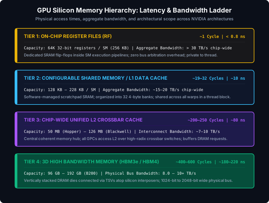 Figure 1: The four-tier GPU memory hierarchy ladder. Latencies, bandwidth capacities, and physical domains across register files, on-chip SRAM, L2 crossbar cache, and 3D High Bandwidth Memory. Source: Architectural hardware specifications adapted from NVIDIA Technical Documentation.
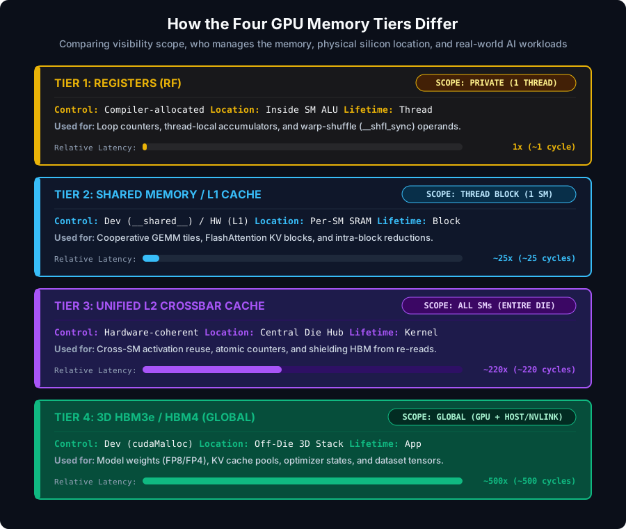 Figure 2: Architectural differences across the four GPU memory tiers—comparing thread/block/chip/global visibility scope, compiler vs. developer vs. hardware control, physical silicon location, relative cycle latency, and typical AI workload usage.
Tier 1: On-Chip Register Files (Sub-Nanosecond Speed)
The Register File is the fastest storage medium on the GPU die, physically embedded directly adjacent to the ALU datapaths inside each Streaming Multiprocessor (SM).
- Latency: ~1 clock cycle (<0.8 nanoseconds).
- Capacity: Typically 64K 32-bit registers per SM (256 KB per SM). Across a 144-SM flagship processor like the Blackwell B200, the aggregate register pool spans over 36 MB of ultra-fast static storage.
- Scope: Registers are private to individual threads. When a kernel launches, the hardware warp scheduler assigns a static slice of registers to each thread for its entire lifecycle.
Tier 2: Configurable Shared Memory & L1 Data Cache (SRAM)
Each SM features a unified pool of high-speed on-chip SRAM that can be configured by the developer into varying ratios of hardware L1 cache and software-managed Shared Memory.
- Latency: ~19 to 32 clock cycles (~10 nanoseconds).
- Capacity: 128 KB (Volta V100) to 228 KB (Hopper H100 / Blackwell B200) per SM.
- Scope: Shared memory is visible to all threads residing within the same Thread Block. It functions as an explicit, software-controlled scratchpad memory that allows threads to cooperate, exchange intermediate values, and stage data cooperatively without touching slower off-chip buses.
Tier 3: Chip-Wide Unified L2 Crossbar Cache
At the chip level, all SMs share a massive, unified Level 2 (L2) cache that sits at the center of the GPU die.
- Latency: ~200 to 250 clock cycles (~80 nanoseconds).
- Capacity: 6 MB (Volta V100), 40 MB (Ampere A100), 50 MB (Hopper H100), and 126 MB (Blackwell B200).
- Scope: The L2 cache is fully coherent across all Graphics Processing Clusters (GPCs). Any data request that misses in an SM’s local L1 cache routes across a high-radix crossbar switch network into the L2 cache, which acts as the primary buffer between compute clusters and external memory controllers.
Tier 4: 3D High Bandwidth Memory (HBM3e / HBM4)
When data is not present in on-chip SRAM or L2 cache, requests must travel off the compute die to the main device memory.
- Latency: ~400 to 600 clock cycles (~150 to 200 nanoseconds).
- Capacity & Bandwidth: Up to 192 GB of HBM3e delivering 8.0 TB/s on Blackwell B200, expanding to over 10 TB/s with next-generation HBM4.
- Scope: Global memory is accessible by every thread across the entire GPU, host CPUs over PCIe or NVLink, and remote GPUs in scale-up clusters.
3. Generational Evolution: How Memory Subsystems Scaled
Over the last decade, GPU memory architectures transitioned from planar PCB circuit traces to 3D stacked silicon. The table below traces this evolution from Volta V100 through Blackwell Ultra (B300 / GB300), Vera Rubin (R200), and the Rubin Ultra roadmap:
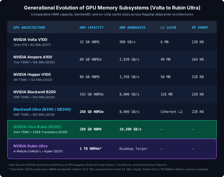 Figure 3: Generational comparison of HBM capacity, physical bandwidth, L2 cache sizing, and per-SM SRAM from Volta V100 to Vera Rubin and Rubin Ultra. Source: NVIDIA Architecture Briefings & Whitepapers, TrendForce, and SemiAnalysis Reports.
Notice two parallel scaling axes:
- On-Chip Cache Expansion: L2 cache capacity expanded by 21× between Volta (6 MB) and Blackwell B200 (126 MB), allowing entire attention tiles and intermediate activations to stay on-chip without hitting external DRAM.
- 3D HBM Stack Density & Bus Speed: Moving from 8-Hi to 12-Hi HBM3e stacks pushed Blackwell Ultra (B300 / GB300) to 288 GB per GPU at 8 TB/s, while Vera Rubin (R200) transitions to HBM4 (288 GB at 19.2 TB/s production bandwidth, more than doubling Blackwell’s bus speed), and Rubin Ultra targets 1 TB of HBM4e on 4-reticle CoWoS-L packaging.
4. Shared Memory Banking & Conflict Mechanics
While Shared Memory delivers blistering bandwidth (over 15 TB/s aggregate across the chip), that throughput is only realized if threads access memory without colliding.
To service 32 threads in a warp simultaneously in a single clock cycle, the hardware divides the shared memory SRAM into 32 independent memory banks, each with a word width of 4 bytes (32 bits):
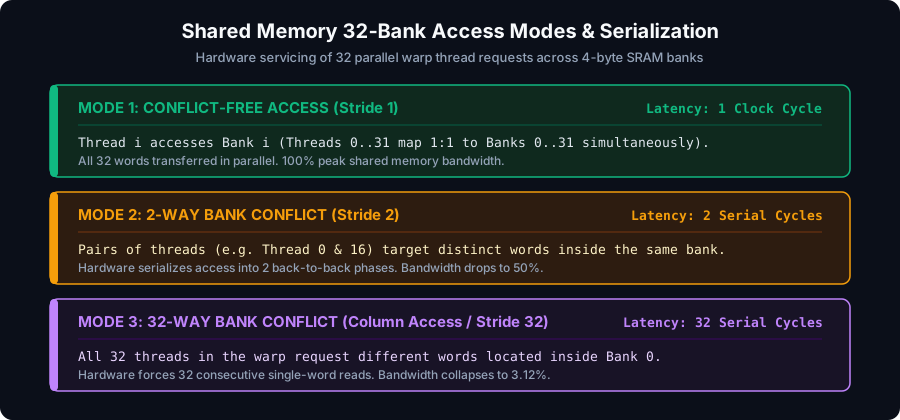 Figure 4: Shared Memory 32-Bank Access Modes. Conflict-free access (1 cycle), 2-way bank conflicts (2 serialized phases), and 32-way catastrophic bank conflicts (32 serialized phases). Source: Conceptual banking architecture adapted from NVIDIA CUDA C++ Programming Guide.
The Bank Conflict Rule
If multiple threads in a warp access different words located within the same physical bank, the memory controller cannot service them in parallel. Instead, the hardware serializes the conflicting requests:
- Conflict-Free (1 cycle): Thread 0 accesses Bank 0, Thread 1 accesses Bank 1, …, Thread 31 accesses Bank 31. All 32 words transfer concurrently in a single clock cycle.
- Broadcast Mode (1 cycle): If multiple threads read the exact same address in the same bank, the hardware broadcasts the word to all requesting threads in a single cycle without conflict.
- N-Way Bank Conflict (N cycles): If 2 threads request different addresses belonging to Bank 4, the transaction becomes a 2-way conflict and takes 2 cycles. In the worst case where all 32 threads request different addresses in the same bank (such as column-wise access in a 32x32 matrix), throughput collapses by 32×, stalling the entire warp for 32 clock cycles.
5. Global Memory Coalescing: The 128-Byte Sector Protocol
When threads read from or write to off-chip global memory, memory requests are handled at the granularity of Warps (32 parallel threads). The GPU memory controller does not fetch individual 4-byte floating-point numbers; it transfers memory in 128-byte cache lines, organized as four 32-byte sectors.
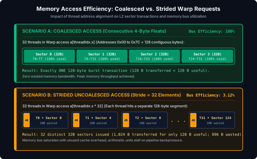 Figure 5: Warp memory transaction efficiency. Coalesced access satisfies all 32 threads with a single 128-byte cache line transaction (100% bus efficiency), whereas strided access triggers 32 separate sector transactions, collapsing bus efficiency to 3.12%. Source: Conceptual memory controller architecture adapted from NVIDIA CUDA Programming Guides.
Scenario A: Coalesced Access (100% Efficiency)
When Thread 0 requests element 0, Thread 1 requests element 1, and so on up to Thread 31, the entire warp requests 32 consecutive 4-byte floats (32 × 4 = 128 contiguous bytes).
- The memory controller checks the base address. Because all requested addresses fall neatly into a single aligned 128-byte boundary, the hardware issues exactly ONE 128-byte transaction.
- Every single byte pulled across the bus is utilized by the application, achieving 100% bus utilization.
Scenario B: Strided Uncoalesced Access (3.12% Efficiency)
Now imagine the algorithm accesses memory with a stride of 32 (for instance, reading down the column of a large non-transposed 2D array):
- Thread 0 reads element 0, Thread 1 reads element 32 (offset 128 bytes), Thread 2 reads element 64 (offset 256 bytes), and so on.
- Because every thread requests a word residing in a completely different cache line, the memory controller is forced to issue 32 distinct 32-byte sector transactions.
- The hardware transfers 1,024 bytes across the memory bus, but the application only consumes 128 bytes. The remaining 896 bytes (96.88%) are discarded as unused cache overhead.
- The memory bus saturates instantly with useless traffic, throttling kernel execution speed to a fraction of hardware capability.
6. Analytical Simulation: GPU Memory Access Coalescing Engine
To quantify the performance penalty of uncoalesced memory access and bank conflicts, the following Python simulation models how a warp’s memory access pattern translates into physical memory transactions and bus efficiency.
Click to expand runnable code script
"""
GPU Memory Subsystem Simulator: Coalescing & Bank Conflict Analyzer.
Models L2 cache sector transactions (32-byte sectors, 128-byte cache lines)
and 32-bank shared memory serialization across 32-thread warps.
"""

from dataclasses import dataclass
from typing import List, Set

WARP_SIZE = 32
SECTOR_SIZE_BYTES = 32
CACHE_LINE_BYTES = 128
SHMEM_BANKS = 32
BANK_WORD_BYTES = 4

@dataclass
class CoalescingResult:
    pattern_name: str
    elements_requested: int
    bytes_useful: int
    sectors_transferred: int
    bytes_transferred: int
    bus_efficiency_pct: float

@dataclass
class BankConflictResult:
    pattern_name: str
    serialization_factor: int
    effective_bandwidth_pct: float

def simulate_global_coalescing(pattern_name: str, addresses: List[int], element_size: int = 4) -> CoalescingResult:
    """Simulates L2 sector transactions for a 32-thread warp memory request."""
    assert len(addresses) == WARP_SIZE

    unique_sectors: Set[int] = set()
    for addr in addresses:
        sector_id = addr // SECTOR_SIZE_BYTES
        unique_sectors.add(sector_id)

    num_sectors = len(unique_sectors)
    bytes_transferred = num_sectors * SECTOR_SIZE_BYTES
    bytes_useful = WARP_SIZE * element_size
    efficiency = (bytes_useful / bytes_transferred) * 100.0 if bytes_transferred > 0 else 0.0

    return CoalescingResult(
        pattern_name=pattern_name,
        elements_requested=WARP_SIZE,
        bytes_useful=bytes_useful,
        sectors_transferred=num_sectors,
        bytes_transferred=bytes_transferred,
        bus_efficiency_pct=efficiency
    )

def simulate_shared_memory_banks(pattern_name: str, addresses: List[int]) -> BankConflictResult:
    """Simulates 32-bank shared memory access for a 32-thread warp."""
    assert len(addresses) == WARP_SIZE

    # Map each thread to bank and word offset
    bank_requests = [set() for _ in range(SHMEM_BANKS)]
    for thread_id, addr in enumerate(addresses):
        word_index = addr // BANK_WORD_BYTES
        bank_id = word_index % SHMEM_BANKS
        bank_requests[bank_id].add(word_index)

    # The max distinct words requested from any single bank determines serialization
    max_conflicts = max(len(words) for words in bank_requests)
    serialization = max(max_conflicts, 1)
    bandwidth_pct = (1.0 / serialization) * 100.0

    return BankConflictResult(
        pattern_name=pattern_name,
        serialization_factor=serialization,
        effective_bandwidth_pct=bandwidth_pct
    )

def main():
    print("=" * 70)
    print("GPU MEMORY SUBSYSTEM SIMULATION: COALESCING & BANK CONFLICTS")
    print("=" * 70)

    # 1. Global Memory Access Patterns (32 threads)
    # Pattern A: Linear Coalesced (a[threadIdx.x])
    linear_addrs = [t * 4 for t in range(WARP_SIZE)]
    res_linear = simulate_global_coalescing("Coalesced (Stride 1)", linear_addrs)

    # Pattern B: Strided access (a[threadIdx.x * 2])
    stride2_addrs = [t * 2 * 4 for t in range(WARP_SIZE)]
    res_stride2 = simulate_global_coalescing("Strided (Stride 2)", stride2_addrs)

    # Pattern C: Heavy Strided access (a[threadIdx.x * 32])
    stride32_addrs = [t * 32 * 4 for t in range(WARP_SIZE)]
    res_stride32 = simulate_global_coalescing("Uncoalesced (Stride 32)", stride32_addrs)

    print("\n[PART 1: GLOBAL MEMORY COALESCING EFFICIENCY]")
    print(f"{'Access Pattern':<26} | {'Sectors':<8} | {'Bytes Sent':<11} | {'Bus Efficiency':<14}")
    print("-" * 70)
    for r in [res_linear, res_stride2, res_stride32]:
        print(f"{r.pattern_name:<26} | {r.sectors_transferred:<8} | {r.bytes_transferred:<11} | {r.bus_efficiency_pct:>6.2f}%")

    # 2. Shared Memory Bank Conflict Patterns
    # Shmem Pattern A: Linear conflict-free (s[threadIdx.x])
    shmem_linear = [t * 4 for t in range(WARP_SIZE)]
    b_linear = simulate_shared_memory_banks("Conflict-Free (Stride 1)", shmem_linear)

    # Shmem Pattern B: Stride 2 (2-way conflict)
    shmem_stride2 = [t * 2 * 4 for t in range(WARP_SIZE)]
    b_stride2 = simulate_shared_memory_banks("2-Way Conflict (Stride 2)", shmem_stride2)

    # Shmem Pattern C: Stride 32 (32-way catastrophic conflict)
    shmem_stride32 = [t * 32 * 4 for t in range(WARP_SIZE)]
    b_stride32 = simulate_shared_memory_banks("32-Way Conflict (Stride 32)", shmem_stride32)

    print("\n[PART 2: SHARED MEMORY BANK CONFLICT SERIALIZATION]")
    print(f"{'Access Pattern':<26} | {'Serialization':<14} | {'Effective Throughput':<20}")
    print("-" * 70)
    for b in [b_linear, b_stride2, b_stride32]:
        print(f"{b.pattern_name:<26} | {b.serialization_factor} cycles        | {b.effective_bandwidth_pct:>6.2f}%")
    print("=" * 70)

if __name__ == "__main__":
    main()
What’s Next in the Series?
Now that we have deconstructed the hardware silicon—from physical transistors and logic gates to Streaming Multiprocessors, Tensor Core systolic arrays, and the nanosecond memory hierarchy—a fundamental question emerges:
How did we go from fixed-function graphics chips designed solely to render 3D triangles to writing general-purpose software running across millions of parallel threads?
In Part 10: The CUDA Revolution I: The Genesis of GPGPU and the Billion-Dollar Gamble, we dive into the origins of general-purpose GPU computing: the dark ages of disguising linear algebra as RGB textures in OpenGL fragment shaders, Ian Buck’s breakthrough with BrookGPU at Stanford, and Jensen Huang’s historic multi-billion-dollar gamble in 2006 that paved the way for modern artificial intelligence.