
From Transistors to Logic Gates: How Physics Turns into Math (CMOS, Adders, and ALUs)
How quantum electron flow becomes arithmetic: MOSFETs to GAAFETs, CMOS static power cancellation, boolean logic, and assembling high-throughput GPU ALUs.
Series: Part 2 of GPU Architecture, Scale-Up Interconnects, and AI Datacenter Infrastructure Series | (Previous) From Sand to Silicon: The Semiconductor Fab, Wafers, Dies, and the Reticle Limit | (Next) What is a GPU and Why Should You Care? (CPU vs. GPU, History, and the Compute Paradigm Shift)
Summary
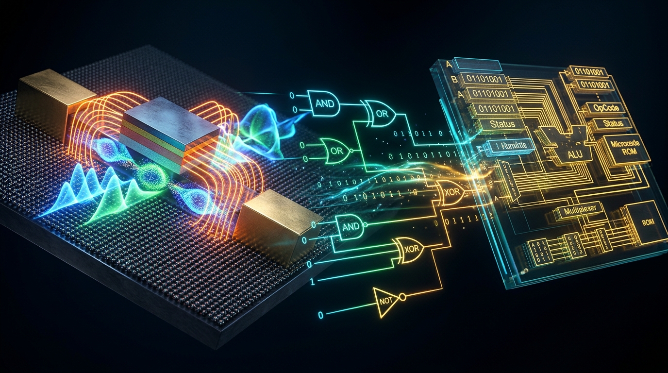
At its physical foundation, a digital computer contains no numbers, matrices, or code. It is a dense sea of silicon dioxide, doped crystal channels, and electrical charge states governed by electromagnetic field potentials. Yet by arranging solid-state switches into complementary pairs, electrical engineers bridge the chasm between raw solid-state physics and abstract discrete mathematics—turning the drift of electrons into addition, subtraction, floating-point multiplication, and neural network tensor contractions.
In Part 2 of our GPU Architecture, Scale-Up Interconnects, and AI Datacenter Infrastructure Series, we trace this mechanical transformation from the atomic scale to the computing pipeline. We deconstruct how MOSFETs, 3D FinFETs, and Gate-All-Around (GAAFET) nanosheets act as sub-nanometer electron valves, why Complementary Metal-Oxide-Semiconductor (CMOS) architecture won digital computing by driving static idle power consumption to near-zero, how cross-coupled transistors build universal boolean logic gates (NAND, NOR, XOR), how half-adders combine into Carry-Lookahead Adders and Arithmetic Logic Units (ALUs), and how modern GPUs orchestrate tens of thousands of these arithmetic engines in parallel to power the artificial intelligence revolution.
Prior Reading Material
To follow the physical hardware journey from raw materials to advanced computing logic, explore these foundational articles:
- From Sand to Silicon: The Semiconductor Fab, Wafers, Dies, and the Reticle Limit — Part 1: Czochralski monocrystalline ingots, 13.5nm EUV photolithography, wafer defect density, and the 858 mm² optical reticle ceiling.
- Silicon at the Edge: NVIDIA Jetson Thor Architecture & Isaac ROS Acceleration — Edge SoC architecture, Neoverse V3AE execution pipelines, and FP4 tensor math.
- Basics of AI Inference: Compute vs Memory Bound — Operational intensity, arithmetic throughput limits, and the arithmetic logic pipeline.
- Inside the Learning Engine: Forward Pass, Backpropagation, and Autograd — How mathematical matrix algebra maps into physical hardware execution.
1. The Electronic Valve: Controlling Electron Channels
A transistor is fundamentally an electronic valve without moving parts. In a hydraulic system, a valve turns a handle to tighten a rubber plunger, physically restricting water flow through a pipe. In a Field-Effect Transistor (FET), an electric voltage applied to a Gate terminal generates an electrostatic field that creates, constricts, or opens a conductive channel of electrons between a Source and a Drain.
flowchart TD
    V1["Gate Voltage Applied (Vg >= Vth)"] --> V2["Electrostatic Field Penetrates Dielectric Oxide Barrier"]
    V2 --> V3["Mobile Minority Charge Carriers Invert Channel Under Gate"]
    V3 --> V4["Low-Resistance Conductive Electron Channel Formed"]
    V4 --> V5["Current (Id) Flows Between Source and Drain Terminals"]
    V5 --> V6["Logic State: Low Impedance (Closed Switch / Digital True)"]

    style V1 fill:#0d2b45,stroke:#00e5ff,stroke-width:2px,color:#ffffff;
    style V2 fill:#0f172a,stroke:#38bdf8,stroke-width:2px,color:#ffffff;
    style V3 fill:#1a3d3c,stroke:#2dd4bf,stroke-width:2px,color:#ffffff;
    style V4 fill:#0f382c,stroke:#10b981,stroke-width:2px,color:#ffffff;
    style V5 fill:#2e1065,stroke:#a855f7,stroke-width:2px,color:#ffffff;
    style V6 fill:#3b0764,stroke:#d946ef,stroke-width:2px,color:#ffffff;
The Transistor Evolutionary Arc: Planar to GAAFET
As silicon fabrication shrunk feature sizes from 180 nm down to 2 nm, quantum mechanical leakage threatened to end computing:
- Planar MOSFET (Legacy to 28nm): A flat gate rests atop a 2D silicon channel. As the gate length shrunk below 25 nm, the gate lost electrostatic control over electrons creeping through the bottom of the channel (source-to-drain subthreshold leakage).
- 3D FinFET (22nm to 3nm): The channel is extruded upward into a vertical 3D “fin,” and the gate wraps around it on three sides. This increased capacitive gate control, drastically slashing subthreshold leakage and enabling the smartphone and Hopper GPU era.
- Gate-All-Around (GAAFET / Nanosheets, 3nm / 2nm): In state-of-the-art TSMC and Intel nodes, the fin is sliced horizontally into stacked parallel silicon ribbons (nanosheets). The gate material completely surrounds the channel on all four sides, maximizing electrostatic grip and preventing quantum tunneling leakage.
2. Why CMOS Won Computing: Complementary Symmetry
In the 1970s, early microprocessors used NMOS logic (such as the famous 6502 and Z80). NMOS used an N-channel transistor paired with a passive pull-up resistor. While simple, NMOS had a fatal flaw: whenever the output was grounded (digital zero), electrical current constantly drained through the resistor directly into ground, dissipating continuous heat even when the computer was idle.
The breakthrough that saved computing from thermal self-destruction is CMOS (Complementary Metal-Oxide-Semiconductor):
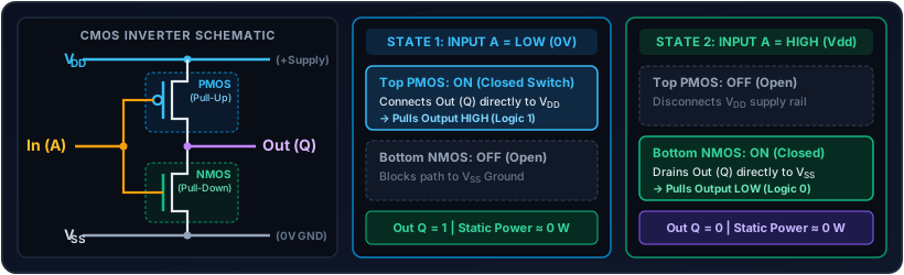 Figure 1. CMOS Inverter schematic and steady-state operating modes: an input voltage drives complementary PMOS and NMOS gates so one switch is always open, ensuring zero static DC path to ground.
CMOS pairs two distinct types of transistors in perfect symmetry:
- NMOS (Pull-Down Network): Conducts when the gate voltage is HIGH (Logic 1), connecting output to Ground (
0V). - PMOS (Pull-Up Network): Conducts when the gate voltage is LOW (Logic 0), connecting output to Supply Voltage (
Vdd).
The Zero Static Power Marvel
When the input to a CMOS inverter is HIGH (Vdd):
- The bottom NMOS turns ON (conducting to Ground).
- The top PMOS turns OFF (open circuit).
- The output is pulled down to
0V(Logic 0).
When the input is LOW (0V):
- The bottom NMOS turns OFF (open circuit).
- The top PMOS turns ON (conducting to
Vdd). - The output is pulled up to
Vdd(Logic 1).
At no point in steady state is there ever a continuous conductive path from Vdd directly to Ground. A CMOS circuit consumes near-zero electrical power when idle. It only consumes energy during the brief picosecond transition when gate capacitance charges or discharges (Dynamic Power = Capacitance × Voltage² × Frequency). This single physical property allowed NVIDIA and TSMC to scale from a few thousand transistors in 1980 to over 208 billion transistors inside an NVIDIA Blackwell B200 package without melting the silicon into slag.
3. Building Universal Logic Gates
By wiring PMOS and NMOS transistors in series or parallel, we construct the fundamental building blocks of Boolean algebra:
flowchart TD
    G1["CMOS Transistor Pairs (PMOS Pull-Up + NMOS Pull-Down)"] --> G2["Universal Inverting Gates: NAND & NOR"]
    G2 --> G3["Non-Inverting Boolean Gates: AND, OR, XOR, XNOR"]
    G3 --> G4["Arithmetic Building Blocks: Half Adders & Full Adders"]
    G4 --> G5["Multi-Bit Arithmetic: Ripple-Carry & Carry-Lookahead Adders"]
    G5 --> G6["Arithmetic Logic Unit (ALU): Add, Sub, Mul, Logic, Comparison"]

    style G1 fill:#0d2b45,stroke:#00e5ff,stroke-width:2px,color:#ffffff;
    style G2 fill:#0f172a,stroke:#38bdf8,stroke-width:2px,color:#ffffff;
    style G3 fill:#1a3d3c,stroke:#2dd4bf,stroke-width:2px,color:#ffffff;
    style G4 fill:#0f382c,stroke:#10b981,stroke-width:2px,color:#ffffff;
    style G5 fill:#2e1065,stroke:#a855f7,stroke-width:2px,color:#ffffff;
    style G6 fill:#3b0764,stroke:#d946ef,stroke-width:2px,color:#ffffff;
Why NAND is Universal
In CMOS physics, inverting gates (NAND and NOR) are faster, smaller, and consume fewer transistors than non-inverting gates (AND and OR). An AND gate is actually built by fabricating a 4-transistor NAND gate followed by a 2-transistor Inverter (6 transistors total).
Because NAND is functionally complete, any mathematical operation known to humanity—from a chess engine to GPT-4o’s attention weights—can be constructed using nothing but interconnected NAND gates.
| Gate Type | Transistor Count | Boolean Expression | Output Truth Table (A=0, B=0 / A=1, B=1) |
|---|---|---|---|
| Inverter (NOT) | 2 Transistors (1P + 1N) | Y = NOT A | Inverts input (0 -> 1, 1 -> 0) |
| NAND Gate | 4 Transistors (2P par, 2N ser) | Y = NOT (A AND B) | Output 0 only when both inputs are 1 |
| NOR Gate | 4 Transistors (2P ser, 2N par) | Y = NOT (A OR B) | Output 1 only when both inputs are 0 |
| AND Gate | 6 Transistors (NAND + NOT) | Y = A AND B | Output 1 only when both inputs are 1 |
| OR Gate | 6 Transistors (NOR + NOT) | Y = A OR B | Output 1 if either input is 1 |
| XOR Gate | 8–12 Transistors | Y = A XOR B | Output 1 if inputs are different |
The Exclusive-OR (XOR) gate is the critical gateway to mathematics: its truth table matches 1-bit binary addition without a carry (0+0=0, 0+1=1, 1+0=1, 1+1=0).
4. From Logic Gates to Arithmetic Computation
How do we take voltage gates and perform arithmetic? We assemble Adders.
The Half Adder
Adding two single-bit binary numbers A and B:
- Sum (
S):S = A XOR B(XOR gate) - Carry-Out (
C):C = A AND B(AND gate)
If A = 1 and B = 1, the Sum is 0 and the Carry is 1, producing the binary output 10 (which equals 2 in decimal).
The Full Adder
A Half Adder cannot handle an incoming carry bit from a preceding column. To chain addition across multiple bits, we build the Full Adder, taking inputs A, B, and Cin:
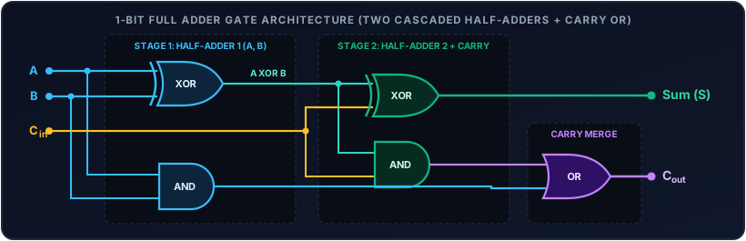 Figure 2. One-bit Full Adder gate architecture: two cascaded Half-Adder stages (XOR + AND) combined with an OR gate to produce the final Sum (
S) and Carry-Out (Cout).
The Boolean logic for the full adder combines two XOR stages for the sum bit and an OR merge for the carry-out:
- Sum (
S):A XOR B XOR Cin - Carry-Out (
Cout):(A AND B) OR (Cin AND (A XOR B))
The Propagation Delay Problem: Ripple vs. Lookahead
If you chain 32 full adders together to add two 32-bit integers (a Ripple-Carry Adder), the 32nd bit cannot compute its sum until the carry signal ripples sequentially through all 31 preceding stages. At 10–20 picoseconds per gate, this ripple latency caps clock frequencies.
To eliminate this bottleneck, modern ALUs use Carry-Lookahead Adders (CLA). By pre-calculating two signals for every bit position in parallel:
- Generate (
G = A AND B): The bit stage generates a carry regardless of any incoming carry. - Propagate (
P = A XOR B): The bit stage passes an incoming carry forward to the next bit.
Because Generate and Propagate depend only on the immediate inputs A and B, the carry for every single bit can be evaluated in parallel across a multi-layer lookahead tree in logarithmic gate delays (O(log N)) rather than linear sequential delays (O(N)).
5. Assembling the Arithmetic Logic Unit (ALU)
Combining a Carry-Lookahead Adder with a bank of Multiplexers (MUX) yields the core workhorse of every CPU and GPU: the Arithmetic Logic Unit (ALU).
An ALU accepts:
- Operand A & Operand B (e.g. two 32-bit binary words).
- Opcode Control Signals (selecting the operation: ADD, SUB, AND, OR, XOR, SHIFT, COMPARE).
- Status Flags (Zero flag
Z, Negative flagN, Overflow flagV, Carry flagC).
flowchart TD
    AL1["Input Operands: 32-bit Register A & Register B"] --> AL2["Opcode Decoder: ADD / SUB / AND / OR / SHIFT"]
    AL2 --> AL3["Parallel Sub-Execution Units: CLA Adder, Barrel Shifter, Logic Matrix"]
    AL3 --> AL4["4-to-1 Multiplexer (MUX) Controlled by Decoded Opcode"]
    AL4 --> AL5["Output Result Bus & ALU Condition Flags (Z, N, V, C)"]
    AL5 --> AL6["Writeback Stage: Register File / SRAM Cache"]

    style AL1 fill:#0d2b45,stroke:#00e5ff,stroke-width:2px,color:#ffffff;
    style AL2 fill:#0f172a,stroke:#38bdf8,stroke-width:2px,color:#ffffff;
    style AL3 fill:#1a3d3c,stroke:#2dd4bf,stroke-width:2px,color:#ffffff;
    style AL4 fill:#0f382c,stroke:#10b981,stroke-width:2px,color:#ffffff;
    style AL5 fill:#2e1065,stroke:#a855f7,stroke-width:2px,color:#ffffff;
    style AL6 fill:#3b0764,stroke:#d946ef,stroke-width:2px,color:#ffffff;
The GPU Connection: The Scale of Millions
While an ultra-fast high-end desktop CPU (like an Intel Core i9 or AMD Ryzen 9) contains roughly 16 to 32 powerful ALUs optimized for single-threaded branch prediction and out-of-order execution, an NVIDIA Blackwell B200 GPU contains over 28,000 parallel CUDA Core ALUs and Tensor Core systolic arrays.
In a GPU, individual ALUs are stripped of complex branch predictors and out-of-order execution buffers. Instead, they are packed into dense Single Instruction, Multiple Threads (SIMT) execution pipelines and systolic matrix-multiply units. When a transformer model executes a matrix multiply during self-attention, tens of thousands of these exact full-adder and multiplier circuits fire simultaneously across every clock cycle, executing over 20 petaflops of FP4 math.
6. Runnable Simulation: Gate-Level Logic & 4-Bit ALU Emulator
To trace how physical logic gates calculate binary addition and ALU operations from scratch, run this standalone Python simulation:
Click to expand runnable code script
#!/usr/bin/env python3
"""
Gate-Level CMOS Logic & 4-Bit ALU Simulator
Demonstrates how transistor-level Boolean logic gates (AND, OR, XOR)
combine into half adders, full adders, and multi-operation ALUs.
"""

def gate_not(a):
    """Simulates a 2-transistor CMOS inverter."""
    return 1 if a == 0 else 0

def gate_and(a, b):
    """Simulates a CMOS NAND + NOT gate pair."""
    return 1 if (a == 1 and b == 1) else 0

def gate_or(a, b):
    """Simulates a CMOS NOR + NOT gate pair."""
    return 1 if (a == 1 or b == 1) else 0

def gate_xor(a, b):
    """Simulates an Exclusive-OR gate from fundamental gates."""
    # A XOR B = (A AND NOT B) OR (NOT A AND B)
    return gate_or(gate_and(a, gate_not(b)), gate_and(gate_not(a), b))

def half_adder(a, b):
    """Adds two 1-bit inputs, producing Sum and Carry."""
    sum_bit = gate_xor(a, b)
    carry_bit = gate_and(a, b)
    return sum_bit, carry_bit

def full_adder(a, b, cin):
    """Adds two 1-bit inputs and an incoming carry bit."""
    # First half-adder
    s1, c1 = half_adder(a, b)
    # Second half-adder with carry-in
    sum_out, c2 = half_adder(s1, cin)
    # Final carry-out
    carry_out = gate_or(c1, c2)
    return sum_out, carry_out

def four_bit_adder(val_a, val_b, cin=0):
    """Chains 4 full adders to compute 4-bit addition."""
    sum_bits = []
    current_carry = cin

    for bit_idx in range(4):
        a_bit = (val_a >> bit_idx) & 1
        b_bit = (val_b >> bit_idx) & 1
        s_bit, current_carry = full_adder(a_bit, b_bit, current_carry)
        sum_bits.append(s_bit)

    # Reassemble integer from bits
    result = 0
    for idx, bit in enumerate(sum_bits):
        result |= (bit << idx)

    return result, current_carry

def alu_4bit(a, b, opcode):
    """
    Simulates a 4-bit Arithmetic Logic Unit (ALU).
    Opcodes:
      00: ADD (A + B)
      01: SUB (A - B via two's complement: A + ~B + 1)
      10: AND (A & B)
      11: XOR (A ^ B)
    """
    a &= 0x0F # Clamp to 4 bits (0-15)
    b &= 0x0F

    if opcode == "ADD":
        res, cout = four_bit_adder(a, b, cin=0)
        return res, cout
    elif opcode == "SUB":
        # Two's complement subtraction: A + (NOT B) + 1
        b_inverted = 0
        for bit_idx in range(4):
            b_bit = (b >> bit_idx) & 1
            b_inverted |= (gate_not(b_bit) << bit_idx)
        res, cout = four_bit_adder(a, b_inverted, cin=1)
        return res, cout
    elif opcode == "AND":
        res = 0
        for bit_idx in range(4):
            res |= (gate_and((a >> bit_idx) & 1, (b >> bit_idx) & 1) << bit_idx)
        return res, 0
    elif opcode == "XOR":
        res = 0
        for bit_idx in range(4):
            res |= (gate_xor((a >> bit_idx) & 1, (b >> bit_idx) & 1) << bit_idx)
        return res, 0
    else:
        raise ValueError(f"Unknown Opcode: {opcode}")

def run_simulation():
    print("=" * 78)
    print("Gate-Level 4-Bit ALU Hardware Simulation (CMOS Truth Tables & Adders)")
    print("=" * 78)
    print(f"{'Opcode':<8} | {'Input A':<10} | {'Input B':<10} | {'Binary Out':<12} | {'Dec Out':<8} | {'Carry Out'}")
    print("-" * 78)

    test_vectors = [
        ("ADD", 5,  3),   # 0101 + 0011 = 1000 (8)
        ("ADD", 9,  7),   # 1001 + 0111 = 0000 (16 with Carry = 1)
        ("SUB", 12, 4),   # 1100 - 0100 = 1000 (8)
        ("SUB", 5,  5),   # 0101 - 0101 = 0000 (0)
        ("AND", 12, 10),  # 1100 & 1010 = 1000 (8)
        ("XOR", 12, 10),  # 1100 ^ 1010 = 0110 (6)
    ]

    for op, a, b in test_vectors:
        res, cout = alu_4bit(a, b, op)
        bin_str = f"{res:04b}"
        print(f"{op:<8} | {a:<10} | {b:<10} | {bin_str:<12} | {res:<8} | {cout}")

    print("=" * 78)
    print("Simulation complete: All arithmetic and boolean logic verified at gate level.")

if __name__ == "__main__":
    run_simulation()
What’s Next
From the quantum physics of electrostatic gate fields to the deterministic arithmetic of carry-lookahead adders, we have witnessed how silicon turns energy into numbers. Yet a collection of adders is not yet a graphics processing unit.
In Part 3, we explore the historical and architectural divergence that changed computing forever: What is a GPU and Why Should You Care? (CPU vs. GPU, History, and the Compute Paradigm Shift).